Electric Lunatic
www.ElectricLunatic.net
TTL SVGA
Video Memory Row Address Generation
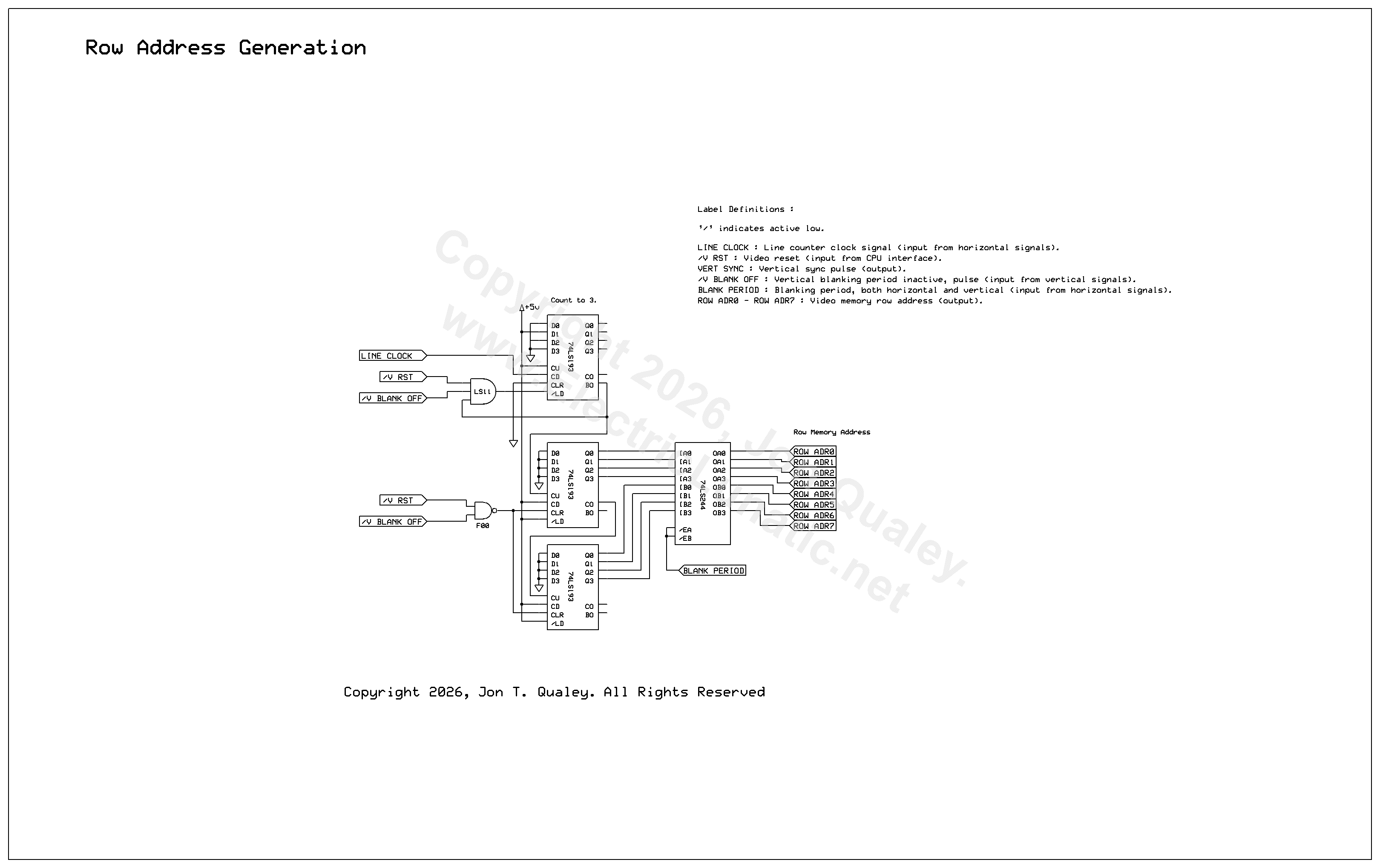
Video Memory Row Address Generator Circuit Schematic
Pixel Generation
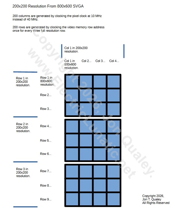
The diagram above shows the relative size of the pixels generated by this circuit compares to the actual pixels in 800 x 600 SVGA mode.
Each pixel generated by this circuit is 4 SVGA mode pixels wide. This is done so that a 10 MHz clock rate can be used to keep access and switching times within the limits of LSTTL and 150 ns static RAM.
Each pixel generated by this circuit is 3 SVGA mode pixels high. This is done so that the pixels look somewhat square. This is also why thge row address circuit increment the video memory row address once per 3 rows.
The video memory addressing scheme is explained in the video memory section.
Row Address Generation Timing
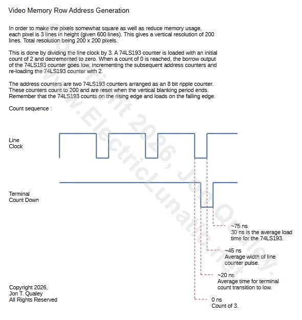
The diagram shown above illustrates the signal timing for row address generation.
Circuit Description
There are three rows of pixels in 800x600 SVGA resolution per one row of pixels displayed by this video adapter. The video memory row address is incremented once per three 800x600 resolution lines. Three 74LS193 counters are used.
The first counter is loaded with 2. Then for each end of a horizontal blanking period labeled LINE CLOCK (the same one used to clock the counters in the vertical signal generator), this counter is decremented.
After three decrements, terminal count (0) is reached and the counter is once again loaded with 2. The terminal count signal also clocks two more 74LS193 counters that generate the video memory row address. The row address is an 8 bit address.
Note that the 74LS244 buffer that drives the row address is in high-Z mode during both horizontal and vertical blanking periods. This is to allow the host CPU to access video memory during the vertical blanking period.
The row address counters are reset at the end of the vertical blanking period.
Copyright 2026, Jon T. Qualey. All Rights Reserved
Back To TTL SVGA