Electric Lunatic
www.ElectricLunatic.net
TTL SVGA
Video Memory
Video Memory and RGB Signals
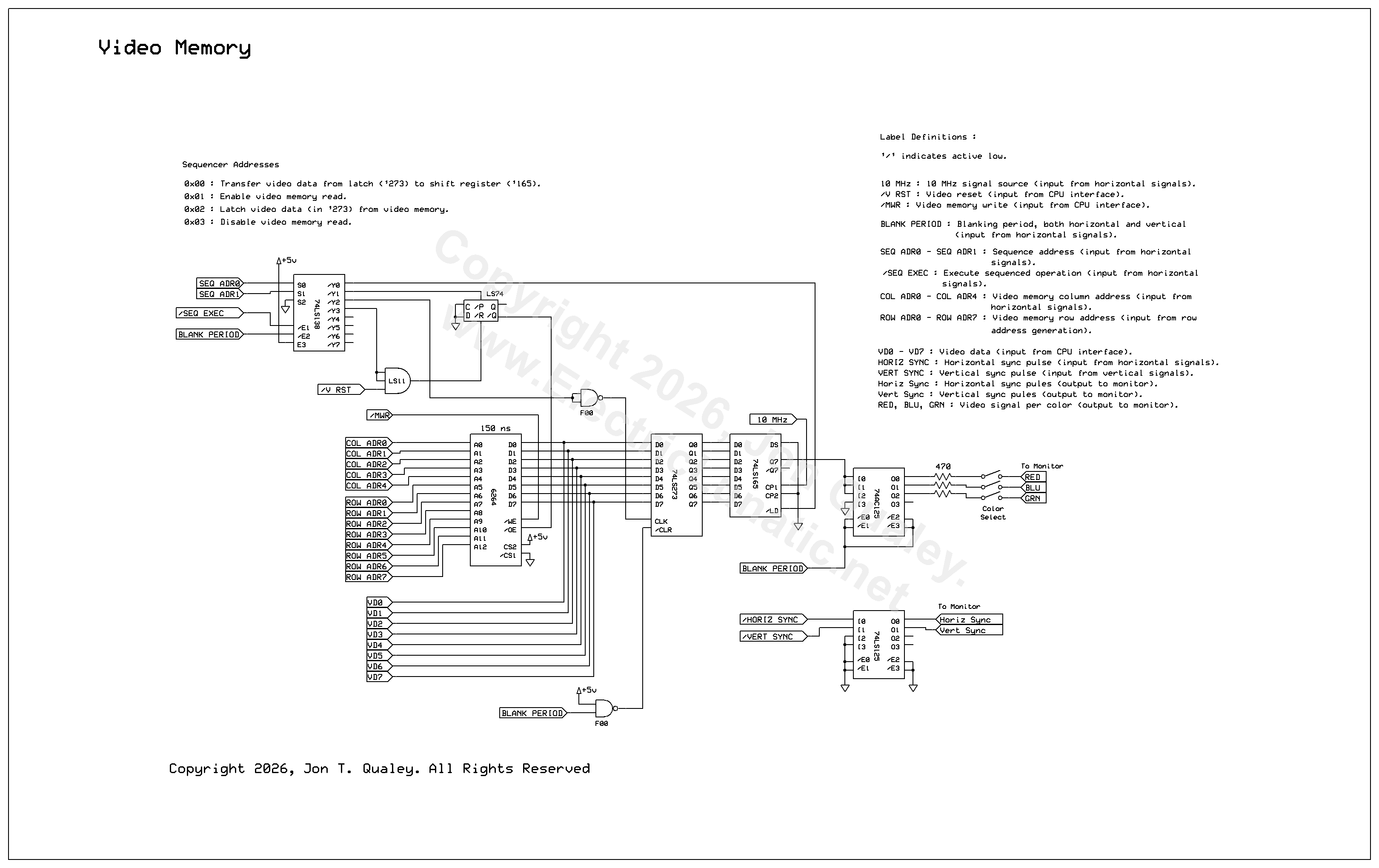
Video Memory Circuit Schematic
Video Memory Address Scheme
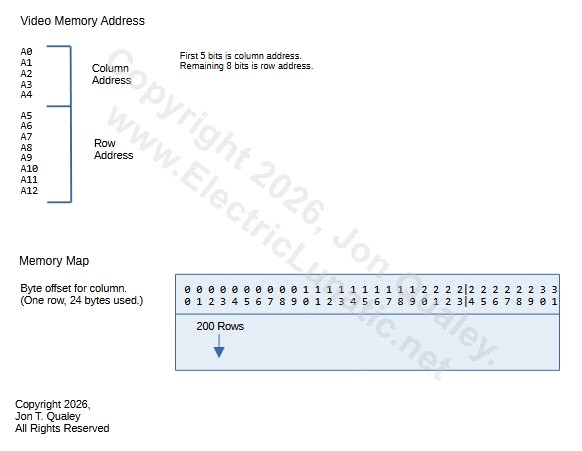
The diagram shown above illustrates the video memory addressing scheme. The 6264 static RAM chip has 13 address lines. The first 5 bits of the address is the column address and the remaining 8 bits of the address is the row address.
There are 200 pixels per row. Each byte stores 8 pixels. 25 bytes are required to store a full row of pixels. However, a 5 bits address is able to access 63 bytes. So 38 bytes per row are not being used at all in the 6264 static RAM device. This is not an efficient use of the memory device, but it does simplify the addressing circuitry. (Yes, the diagram states 24 bytes used because only 24 out of 25 can be accessed and are visible.)
Video Memory Timing
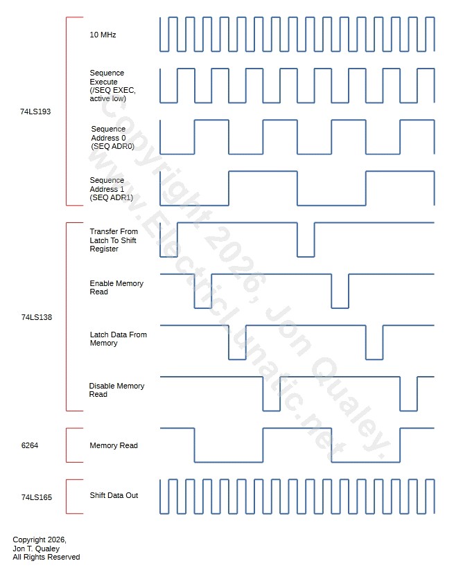
The diagram shown above illustrates the signal timing inside the video memory in relation to each device.
Circuit Description
Data is read from video memory one byte at a time. This will render 8 pixels, one per bit. The byte read from video memory is loaded into a 74LS165 shift register and shifted out at 10 MHz to generate the RGB video signal. The 6264 static RAM used for video memory is not fast enough to load the shift register without double buffering. For this reason, a 74LS273 latch is loaded from video memory and then the shift register is loaded from the latch.
The effect of this double buffering technique is that the first 8 pixels in each row cannot be displayed. At the end of every row, the 74LS273 latch is cleared at the beginning of the horizontal blanking period. If the latch were not cleared, the last 8 pixels displayed will appear as the first 8 pixels in the next row. This limits the horizontal resolution to 192 pixels.
A 74LS138 is used as a sequencer utilizing the /SEQ EXEC, SEQ ADR0 and SEQ ADR1 signals. The 74LS165 shift register is clocked at 10 MHz while sequenced events (/SEQ EXEC) is clocked at 5 MHz. This way, two bits are shifted out to the RGB stream for each of the four sequencer cycles. The last bit in the shift register is clocked out before the shift register is loaded as the shift clock is active high and the /SEQ EXEC signal is active low.
The one exception to using exclusively 74LS and 74F ICs is the RGB signal driver. This is a 74AC125. The 74AC125 was chosen because the noise and overshoot generated by a 74LS125 gives a jagged and sparkly appearance to the pixels displayed. The 74AC125 produces a much cleaner signal giving each pixel a well defined and consistent appearance.
The video memory does not store color information but the color of the video signal can be controlled using the color select switches on each individual RGB line to the monitor.
Video Memory Read Sequence
The memory read sequence is :
- Load the 74LS165 shift register from the 74LS273 latch.
- Read the addressed byte from the 6264 video RAM and hold the read active using an RS flip-flop.
- Load the 74LS273 latch from video RAM.
- Release the read signal on the video RAM.
Data is being shifted out of the shift register whilke the sequence described above is executed.
The diagrams below illustrate the memory read sequence and generation of the RGB signal.
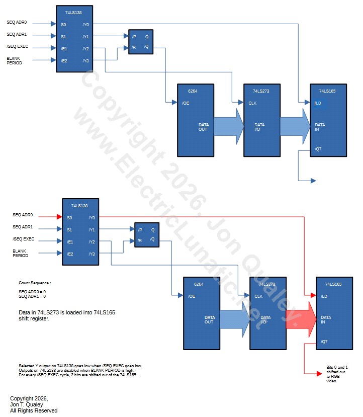
In the diagram image above, the initial state is shown first. In the next diagram, the 74LS165 shift register is loaded with a byte from the 74LS273 latch while the first two bits are shifted out to RGB.
The shift register cannot be loaded while shifting out data. The load is actually interleaved with the shifting operation. The signals on SEQ ADR0, SEQ ADR1, /SEQ EXEC and the 10MHz signal are a simple binary count sequence with the 10Mhz signal (being used to shift the data out of the shift register) being the LSB. Since /SEQ EXEC (which activates the shift register load) is active low and out of phase with the shift operation so it does not interfere with shifting data out of the shift register. The diagram does not illustrate this.
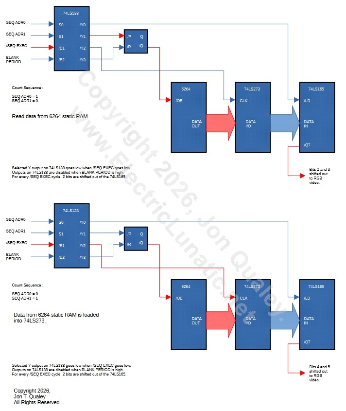
In the diagram image above, The first diagram, a byte from video memory is read and made available to the 74LS273 latch while two more bits are shifted out to RGB. In the next diagram, the 74LS273 latch is loaded while the next two bytes are shifted out to RGB.
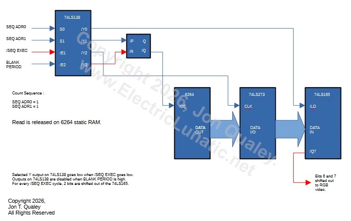
In this diagram the memory read is released while the final two bits are shifted out to RGB.
Copyright 2026, Jon T. Qualey. All Rights Reserved
Back To TTL SVGA